Features
High Performance, Low Power AVR® 8-Bit Microcontroller Family
• Advanced RISC Architecture
– 131 Powerful Instructions
– Most Single Clock Cycle Execution
– 32 x 8 General Purpose Working Registers
– Fully Static Operation
– Up to 20 MIPS Throughput at 20MHz
– On-Chip 2-Cycle Multiplier
• High Endurance Non-Volatile Memory Segments
– 32KBytes of In-System Self-Programmable Flash program memory
– 1KBytes EEPROM
– 2KBytes Internal SRAM
– Write/Erase Cycles: 10,000 Flash/100,000 EEPROM
– Data retention: 20 years at 85°C
– Optional Boot Code Section with Independent Lock Bits
• In-System Programming by On-chip Boot Program
• True Read-While-Write Operation
– Programming Lock for Software Security
• Special Microcontroller Features
– Power-On Reset and Programmable Brown-Out Detection
– Internal 8 MHz Calibrated Oscillator
– External and Internal Interrupt Sources
– Six Sleep Modes: Idle, ADC Noise Reduction, Power-save, Power-down, Standby, and Extended Standby
– Clock Failure Detection Mechanism and Switch to Internal 8 MHz RC Oscillator in case of Failure
– Individual Serial Number to Represent a Unique ID
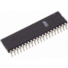
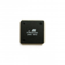
• I/O and Packages
– 27 Programmable I/O Lines
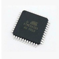
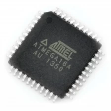
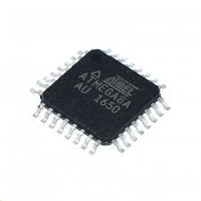
– 32-pin TQFP and 32-pin QFN/MLF
• Operating Voltage: – 1.8 - 5.5V
• Temperature Range: – -40°C to 105°C
• Speed Grade:
– 0 - 4MHz @ 1.8 - 5.5V
– 0 - 10MHz @ 2.7 - 5.5.V
– 0 - 20MHz @ 4.5 - 5.5V
• Power Consumption at 1MHz, 1.8V, 25°C
– Active Mode: 0.24mA
– Power-Down Mode: 0.2μA
– Power-Save Mode: 1.3μA (Including 32kHz RTC)
The pico Power ATmega328PB is a low-power CMOS 8-bit microcontroller based on the AVR enhanced RISC architecture. By executing powerful instructions in a single clock cycle, the ATmega328PB achieves throughputs close to 1MIPS per MHz. This empowers system designers to optimize the device for power consumption versus processing speed.
An 8-bit low-power CMOS microprocessor built on the AVR improved RISC architecture is called the ATmega328PB. The ATmega328PB reaches throughputs near to 1MIPS per MHz by processing strong instructions in a single clock cycle. This gives system designers the ability to balance the device's power use and processing performance. 32 general purpose working registers are combined with a comprehensive instruction set in the core. All 32 registers are directly coupled to the Arithmetic Logic Unit (ALU), enabling simultaneous access to two separate registers during a single clock cycle. In comparison to traditional CISC microcontrollers, the resultant design is quicker and more code-efficient.
Technology for high density non-volatile memory is used to create the device. Through an SPI serial interface, a typical nonvolatile memory programmer, or an On-chip Boot software running on the AVR core, the On-chip ISP Flash enables In-System reprogramming of the programme memory. The application software in the Application Flash memory can be downloaded by the Boot programme via any interface. The Application Flash part will be updated while the software in the Boot Flash area is still operating, enabling real Read-While-Write functioning. The ATmega328PB is a potent microcontroller that offers a highly versatile and economical solution to many embedded control applications by combining an 8-bit RISC CPU with In-System Self-Programmable Flash on a monolithic device.
3rd Floor, 3c , Manek Chambers, above vasant bhuvan, LAMINGTON ROAD, GRANT ROAD,, Mumbai 400007