
32 general purpose working registers are combined with a robust instruction set in the Atmel AVR core. Since each of the 32 registers is directly coupled to the ALU, two separate registers may be accessed in a single instruction that is executed in a single clock cycle. In comparison to traditional CISC microcontrollers, the resultant design is quicker and more code-efficient.
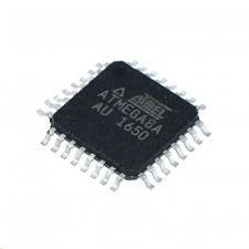
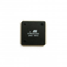
The following capabilities are offered by the ATmega16A: 32 general purpose I/O lines, 32 general purpose working registers, a JTAG interface for boundary-scan, on-chip programming support, three flexible Timer/Counters with compare modes, internal and external interrupts, a serial programmable USART, a byte-oriented Two-wire Serial Interface, an 8-channel, 10-bit ADC with optional different sampling rates, and 16Kbytes of in-system programmable flash programme memory with read-while-write capabilities.
The USART, Two-wire interface, A/D Converter, SRAM, Timer/Counters, SPI port, and interrupt system may all continue to operate when the CPU is in idle mode. The Oscillator is frozen in the Power-down mode, but the register values are saved. Until the next External Interrupt or Hardware Reset, all chip operations are disabled. While the rest of the device is resting in power-save mode, the Asynchronous Timer keeps running, enabling the user to maintain a timer basis. To reduce switching noise during ADC conversions, the ADC Noise Reduction mode turns down the CPU and all other I/O modules except the Asynchronous Timer and ADC. While the rest of the device is sleeping in standby mode, the crystal/resonator oscillator is operating. As a result, highly quick startup and low power consumption are both possible.
3rd Floor, 3c , Manek Chambers, above vasant bhuvan, LAMINGTON ROAD, GRANT ROAD,, Mumbai 400007